Samsung Display Direct-emission OLED Microdisplay: Complete Overview
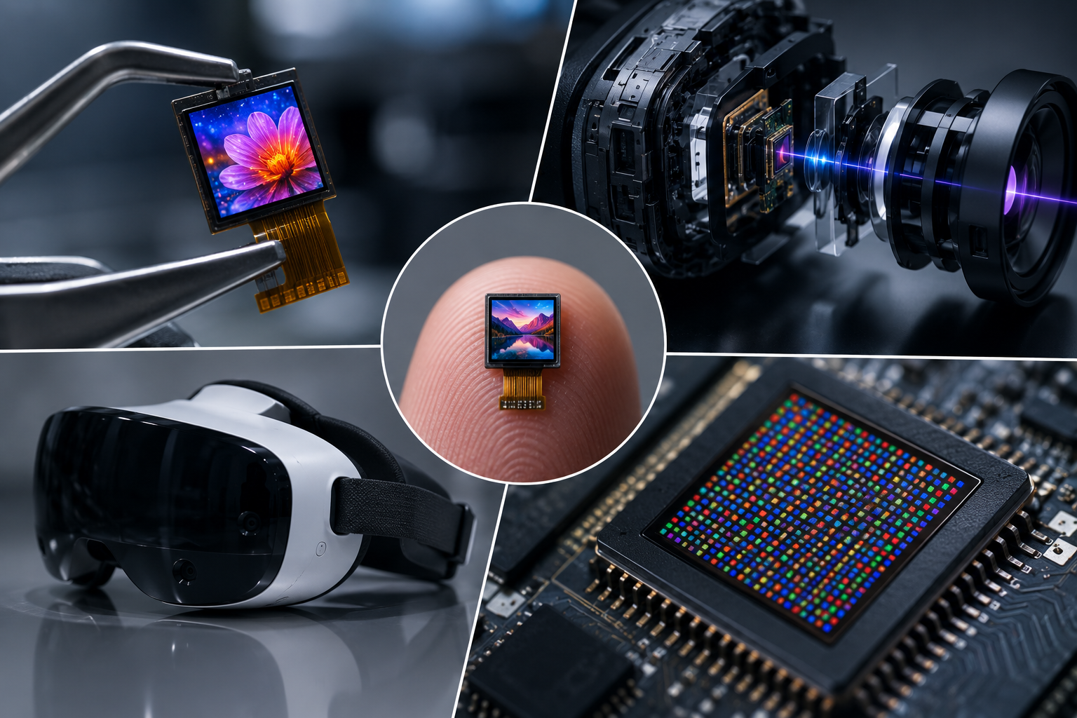
Why Samsung’s Direct-Emission OLED Microdisplay Matters for Your Next Display Investment
If you are responsible for sourcing display modules for AR/VR headsets, medical imaging devices, or industrial HUD systems, the recent announcement from Samsung Display should be on your radar. Industry reports confirm that Samsung has demonstrated a direct-emission OLED microdisplay reaching approximately 40,000 nits — an extreme luminance milestone that pushes brightness into a range previously reserved for specialized HUD and headlight applications. This is not an incremental improvement; it represents a fundamental shift in what is physically possible for near-eye display applications.
For procurement directors and hardware engineers, this development signals a critical inflection point. The display supply chain is about to see a new class of high-resolution microdisplays that could redefine product roadmaps. Understanding the technology, its timeline, and its limitations will help you make informed sourcing decisions today — rather than reacting to market shifts later.
Background: Decoding the Direct-Emission OLED Microdisplay
What Is a Direct-Emission OLED Microdisplay?
Before analyzing the implications, it is essential to clarify the technology. A direct-emission OLED microdisplay builds the OLED emissive layer directly on a silicon backplane (CMOS wafer). Unlike traditional LCD modules that require a backlight and color filters, each pixel in a direct-emission OLED generates its own light. This architecture enables extremely high pixel densities because the pixel circuit is fabricated using semiconductor lithography rather than conventional display patterning.
The “direct-emission” distinction is important. It differentiates this approach from other microdisplay technologies like LCOS (liquid crystal on silicon) or DLP, which rely on external light sources. It also contrasts with white-OLED-plus-color-filter designs, where a white OLED layer is paired with RGB color filters. Direct-emission OLED deposits red, green, and blue emitters individually at the pixel level, allowing for better color purity and efficiency at ultra-high resolutions.
The 40,000-Nit Brightness Milestone
Samsung Display’s demonstration of a 40,000-nit direct-emission OLED microdisplay is remarkable because it shatters the brightness ceiling that most industry analysts considered achievable for near-eye panels. For context, most OLED microdisplays today operate in the 1,000 to 5,000-nit range, with some reaching 10,000 nits. The 40,000-nit figure — roughly 4 to 8 times brighter — directly addresses the “see-through washout” problem in AR optics, where the display must overlay content on a sunlit real-world scene. In terms of resolution, the demonstrated panels (around 1.03 inches) run at roughly 3,500 PPI, comparable to other premium OLED-on-silicon microdisplays.
This achievement is not purely academic. It addresses one of the persistent challenges in AR displays: maintaining legible overlays in bright ambient light. At 40,000 nits, the microdisplay has enough headroom to survive the light loss of waveguides and combiners while remaining visible in daylight — enabling see-through AR and HUD applications that were previously brightness-limited. Combined with a pixel density around 3,500 PPI, which already eliminates the visible “screen-door effect,” this means future AR/VR products could deliver far more convincing visual experiences — with direct implications for training simulations, remote surgery, and industrial maintenance applications.
Key Technical Attributes
- Silicon backplane: Uses CMOS wafers for pixel addressing, enabling high transistor density and precise current control
- RGB direct patterning: Emits red, green, and blue light from dedicated sub-pixels for superior color gamut
- High brightness potential: OLED direct emission allows for efficient light output, critical for see-through AR optics
- Fast response time: Microsecond-level response suited for high-frame-rate content without motion blur
Current Industry Context: Where Does This Fit in the Microdisplay Landscape?
Competitive Landscape
Samsung Display is not alone in the microdisplay race. Sony has been shipping OLED microdisplays for years, and BOE, eMagin, and others are actively developing similar technologies. However, the 40,000-nit figure positions Samsung at the leading edge of brightness. Analysts suggest that most commercially available OLED microdisplays today range from 1,000 to 5,000 nits, with some prototypes reaching 10,000-15,000 nits. Samsung’s demonstration effectively multiplies the brightness envelope by a factor of 3 to 4, a leap that will pressure the rest of the supply chain to respond.
This competitive pressure matters for buyers. When a tier-one manufacturer like Samsung Display pushes the boundary, it forces the entire supply chain to respond. Panel makers, driver IC suppliers, and module assemblers will need to adapt their processes. For OEMs, this means more options will emerge over the next 12-24 months — but it also means early adopters will need to evaluate technologies carefully before committing to long production runs.
Supply Chain and Manufacturing Readiness
The path from demonstration to volume production is rarely short. Direct-emission OLED microdisplays require specialized fabrication facilities capable of handling both OLED deposition and semiconductor lithography. This convergence of display and semiconductor manufacturing is a significant barrier to entry. Industry observers note that yield rates at such extreme pixel densities remain a challenge, and cost-per-module is expected to be substantial in the early production phase.
For B2B procurement teams, this translates into a practical concern: availability. If your product roadmap depends on a 40,000-nit microdisplay, you may face limited supply and premium pricing for the foreseeable future. A pragmatic approach involves designing for scalability — specifying a microdisplay that meets current performance requirements while leaving headroom for future upgrades as the technology matures.
Market Timing and Adoption Signals
The timing of Samsung’s demonstration is notable. AR/VR headset shipments have been growing steadily, and industrial applications — from remote field service to medical training — are expanding. Industry reports suggest that microdisplay demand is projected to grow significantly over the next five years, driven by both consumer and enterprise applications. Samsung’s move signals confidence in this trajectory, and buyers should interpret it as a long-term commitment to the category.
Implications for B2B Display Procurement
Rethinking Product Roadmaps
If your company designs near-eye display systems, the emergence of high-PPI direct-emission OLED microdisplays should influence your roadmap discussions. Products that were previously constrained by display resolution — such as compact AR glasses with wide field-of-view — may now have a viable path forward. However, it is equally important to recognize that high PPI alone does not solve every challenge. Field-of-view, brightness, power consumption, and optical design remain critical variables that interact with pixel density.
Evaluating Total Cost of Ownership
Direct-emission OLED microdisplays are likely to command a premium in the near term. Procurement decisions should account for total cost of ownership, not just unit price. Consider factors like:
- Yield and fallout rates: Higher PPI panels may have lower yields, affecting supply reliability
- Driver IC complexity: Ultra-high-resolution panels require advanced driver circuitry, which impacts BOM cost
- Optical system requirements: The display is only one component; the optics that magnify it must be designed to match its resolution
- Thermal management: Dense OLED arrays generate heat that must be managed in compact enclosures
Balancing Innovation with Risk
It is tempting to chase the latest specification, but B2B procurement is about risk management. A 40,000-nit microdisplay is impressive, but if your application requires high brightness with proven reliability and wide temperature tolerance, a more mature technology may serve you better. The key is to match the display to the application requirements — not to the headline specification.
This is where a knowledgeable display partner becomes valuable. A manufacturer with deep experience across LCD, TFT, and emerging microdisplay technologies can help you assess trade-offs objectively. They can also provide realistic timelines for technology adoption based on supply chain readiness.
How Relialink Helps Buyers Navigate This Evolving Landscape
Independent, Application-Focused Guidance
As a professional LCD module manufacturer, Relialink does not manufacture OLED microdisplays at the 40,000-nit level. We believe in being transparent about that. Our value lies in helping buyers make sense of the broader display ecosystem and selecting the right technology for their specific application.
For many industrial, medical, and automotive applications, high-quality TFT LCD modules remain the most cost-effective and reliable choice. Our expertise covers the full range of display technologies — from standard TFT to specialized high-brightness and wide-temperature modules. When a client comes to us asking about OLED microdisplays, we help them evaluate whether the technology genuinely fits their requirements or whether a well-engineered LCD module delivers better value.
Customization and Integration Support
Display procurement is rarely about picking a standard part off a shelf. Most B2B applications require customization — whether that is an unusual aspect ratio, a specific interface (LVDS, MIPI, RGB), or enhanced optical bonding for outdoor readability. Relialink’s manufacturing capabilities are built around this reality. We work with clients to define specifications, prototype modules, and scale to production volumes with consistent quality.
Our team stays current on display technology trends precisely so we can advise clients on when to adopt new technologies and when to stick with proven solutions. The decision to move from LCD to OLED microdisplay is not one to take lightly; it involves significant redesign, re-qualification, and supply chain changes. We help you navigate that decision with clear-eyed analysis.
Supply Chain Transparency
One of the most underappreciated aspects of display procurement is supply chain stability. When a new technology like direct-emission OLED microdisplay enters the market, supply can be volatile. Relialink maintains strong relationships across the panel supply chain, allowing us to provide reliable lead times and consistent quality — even when the broader market is in flux.
Actionable Next Steps: Selection Criteria for Microdisplay and LCD Decisions
Step 1: Define Your Application Requirements Quantitatively
Before evaluating any display technology, document your requirements in measurable terms:
- Resolution and pixel density: What is the minimum PPI your application truly needs?
- Brightness: What ambient light conditions will the display operate in?
- Viewing angle: Is a wide viewing angle critical, or is the display viewed straight-on?
- Temperature range: Will the display operate in extreme environments?
- Interface and power: What are your system constraints for connectivity and power consumption?
- Lifetime and reliability: What are the expected operating hours and MTBF targets?
Step 2: Compare Technologies Against Requirements
Create a comparison matrix that evaluates LCD, OLED, and microdisplay options against your requirements. Be honest about trade-offs. For example, OLED microdisplays excel in pixel density and contrast, but LCD modules often win on cost, brightness, and availability. The right choice depends on your specific use case.
Step 3: Engage a Display Partner Early
Do not wait until your design is finalized to bring in display expertise. Engage with a manufacturer like Relialink during the concept phase. We can provide feasibility feedback, suggest alternative approaches, and flag potential supply chain issues before they become costly problems.
Step 4: Plan for Technology Evolution
Design your product with flexibility in mind. If a higher-resolution microdisplay becomes available in two years, can your system accommodate it? Modular design approaches — separating the display from the optical system and main board — can future-proof your product and extend its lifecycle.
Step 5: Validate with Prototypes
Specifications on paper are useful, but nothing replaces physical validation. Request sample modules, test them in your actual use environment, and measure performance against your requirements. This step is non-negotiable for mission-critical applications.
Final Thoughts: The Display Landscape Is Evolving — Stay Informed, Stay Flexible
Samsung Display’s direct-emission OLED microdisplay demonstration is a significant milestone that signals where the display industry is heading. For B2B buyers, it is both an opportunity and a cautionary tale. The opportunity is clear: higher resolution displays will enable new product categories and improved user experiences. The caution is equally clear: emerging technologies take time to mature, and the smartest procurement strategies balance innovation with reliability.
The most successful display buyers are those who understand that technology selection is a strategic decision — not a specification exercise. By staying informed about industry developments, partnering with knowledgeable manufacturers, and maintaining flexibility in your design approach, you can navigate this evolving landscape with confidence.
Peak vs. Sustained Brightness: Reading the 40,000-Nit Spec Correctly
Before you design around the headline number, qualify it: industry reports suggest that 40,000 nits is the peak luminance under pulsed drive conditions, not sustained operation. In a real wearable device, thermal management, power budgets, and lifetime requirements will force the actual operating brightness significantly lower. For B2B buyers, the relevant metric is the sustained usable brightness within a product’s thermal and power envelope — and here the trade-offs between OLED microdisplays and LCDs are instructive:
- Brightness — peak vs. sustained. High-performance LCD microdisplays using advanced backlight units achieve 10,000-30,000 nits in pulsed mode and 5,000-10,000 nits sustained. LCDs dissipate heat more evenly across the panel, while OLEDs concentrate heat in the emissive layers — limiting sustained brightness. For continuous high brightness (industrial AR headsets in warehouses or field service), LCD often maintains a practical advantage.
- Color gamut. OLED microdisplays inherently exceed 100% DCI-P3 because each sub-pixel emits its own colored light. LCDs rely on color filters that absorb a portion of the backlight, but premium LCD microdisplays with quantum-dot enhancement films now reach 90-95% DCI-P3 — close enough that the gap only matters for color-critical medical or design review applications.
- Lifetime. This is where LCD pulls ahead decisively. OLED microdisplays suffer differential aging — blue materials degrade faster than red and green — and the high drive currents needed for extreme brightness accelerate it. Industry estimates suggest OLED microdisplays operating at high brightness may show noticeable color shift after 5,000-10,000 hours. LCD microdisplays have no emissive material degradation; backlights can be designed for 30,000-50,000 hours.
- Power consumption. At equivalent brightness, OLED can be more power-efficient because black pixels consume no power. But at the high average brightness levels common in see-through AR, OLED’s efficiency advantage erodes — LCD’s efficient backlight systems can achieve lower total power for bright, high-duty-cycle content.
Five questions every buyer should ask: What sustained brightness does your environment actually require (do not design for peak specs)? What is your target product lifetime, and does the display technology degrade within that window? What is your total BOM cost target (including heat sinking or active cooling for OLED)? What is the realistic supply chain and lead-time risk for the chosen technology? And which optical design does your form factor allow — OLED’s thinness or LCD’s thermal headroom?
Looking for a reliable display partner to help you evaluate your options — whether that means a proven TFT LCD module or guidance on emerging microdisplay technologies? Contact Relialink today to discuss your specific requirements and get expert advice tailored to your application.
Related Reading
- OLED Microdisplay Hits 150,000 Nits: What It Means for LCD Module Selection — INT Tech’s parallel brightness milestone; two technology routes are both pushing the near-eye brightness envelope.
- Supplier profile series: JDI Display Fab: Complete Overview · LG Display OLED Display LCD: Complete Overview · Samsung Display IT AMOLED IT OLED: Complete Overview · Visionox AMOLED: Complete Overview